
An-Chen Liu, Po-Tsung Tu, Catherine Langpoklakpam, Yu-Wen Huang, Ya-Ting Chang, An-Jye Tzou, Lung-Hsing Hsu, Chun-Hsiung Lin, Hao-Chung Kuo and Edward Yi Chang
Micromachines 2021, 12(7), 737 — Published in June 2021
ABSTRACT
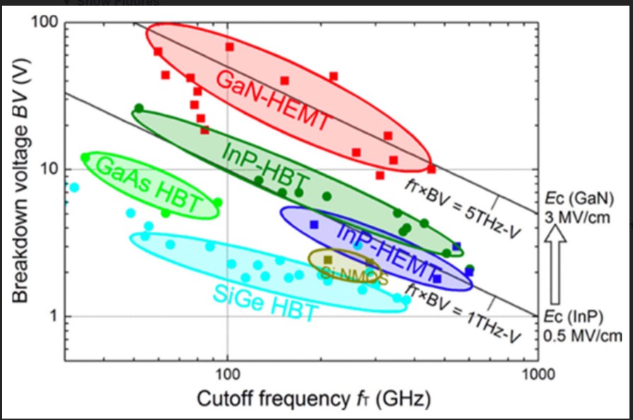
GaN has been widely used to develop devices for high-power and high-frequency applications owing to its higher breakdown voltage and high electron saturation velocity. The GaN HEMT radio frequency (RF) power amplifier is the first commercialized product which is fabricated using the conventional Au-based III–V device manufacturing process. In recent years, owing to the increased applications in power electronics, and expanded applications in RF and millimeter-wave (mmW) power amplifiers for 5G mobile communications, the development of high-volume production techniques derived from CMOS technology for GaN electronic devices has become highly demanded. In this article, we will review the history and principles of each unit process for conventional HEMT technology with Au-based metallization schemes, including epitaxy, ohmic contact, and Schottky metal gate technology. The evolution and status of CMOS-compatible Au-less process technology will then be described and discussed. In particular, novel process techniques such as regrown ohmic layers and metal–insulator–semiconductor (MIS) gates are illustrated. New enhancement-mode device technology based on the p-GaN gate is also reviewed. The vertical GaN device is a new direction of development for devices used in high-power applications, and we will also highlight the key features of such kind of device technology.