
Yuan Lin, Min-Lu Kao, You-Chen Weng, Chang-Fu Dee, Shih-Chen Chen, Hao-Chung Kuo, Chun-Hsiung Lin and Edward-Yi Chang
Micromachines, 13(12), 2140(2022) — Published in December 2022
ABSTRACT
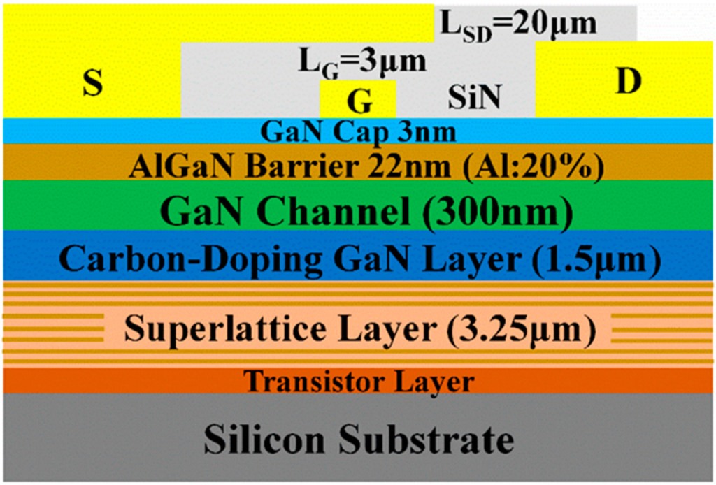
Substrate voltage (VSUB) effects on GaN-on-Si high electron mobility transistors (HEMTs) power application performance with superlattice transition layer structure was investigated. The 2DEG conductivity and buffer stack charge redistribution can be affected by neutral/ionized donor and acceptor traps. As the donor/acceptor traps are excessively ionized or de-ionized by applying VSUB, the depletion region between the unintentionally doped (UID)/Carbon-doped (C-doped) GaN layer may exhibit a behavior similar to the p–n junction. An applied negative VSUB increases the concentration of both the ionized donor and acceptor traps, which increases the breakdown voltage (BV) by alleviating the non-uniform distribution of the vertical electric field. On the other hand, an applied positive VSUB causes the energy band bending flattener to refill the ionized traps and slightly improves the dynamic Ron degradation. Moreover, the amount of electrons injected into the buffer stack layer from the front side (2DEG channel/Ohmic contact) and the back side (AlN nucleation layer/superlattice transition layer) are asymmetric. Therefore, different VSUB can affect the conductivity of 2DEG through the field effect, buffer trapping effect, and charge redistribution, which can change the electrical performance of the device.