
Xiao-Ying Zhang, Yue Yang, Wei-Hang Fan, Chen Wang, Wan-Yu Wu, Ming-Chun Tseng, Dong-Sing Wuu, Peng Gao, Hao-Chung Kuo, Shui-Yang Lien & Wen-Zhang Zhu
Surface and Coatings Technology, 128252 (2022) —Published in February 2022
ABSTRACT
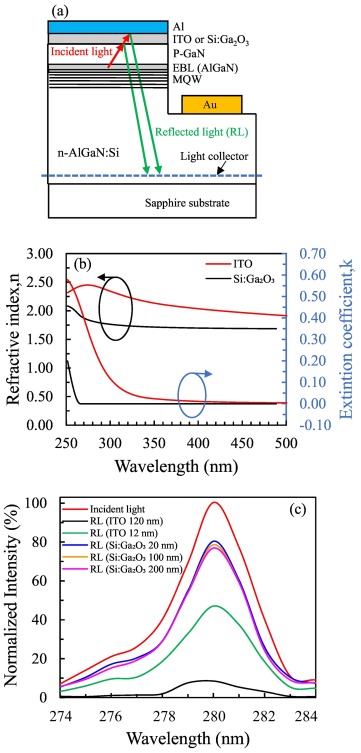
Si-doped Ga2O3 films were prepared on quartz and silicon substrates using remote plasma atomic layer deposition with trimethylgallium, Bis(diethylamino)silane and O2 plasma as the precursors. Different Si-doped concentration in films were obtained by adjusting the numbers of SiO2 circulation ratio. The effect of Si-doped concentration from 0 to 20% on the qualities of the Ga2O3 thin films were studied. The experimental results showed that Ga2O3 thin film growth per cycle increases slightly with the various cycle ratio at the same total cycles of about 600. Field emission scanning electron microscopy shows that the Ga2O3 films have very smooth surface. The spectroscopic ellipsometry tests showed that the refractive index of the Si-doped Ga2O3 thin films decreases monotonically with the doping level increases. The transmittances of all the doped Ga2O3 films are exceed 90% in the visible region. The (400) preferred orientation Ga2O3 thin films were obtained after annealing at 900 °C in N2 atmosphere. Moreover, the x-ray photoelectron spectroscopy investigation indicates that the doped Ga2O3 thin films is Ga-rich with the states of Ga3+ and Ga1+. High resolution transmission electron microscopy mapping measurement shows that the Si composition in the Ga2O3 thin films is uniform. Hall effect measurements demonstrated that the carrier concentration and mobility of the doped Ga2O3 films increase while the resistivity of the films decreases as the Si-doped concentration increases. The results of Si-doped Ga2O3 thin film with 20% cycle ratio shows high transmittance of 93% at 280 nm wavelength and low resistivity of 3.41 Ω·cm. Optical simulations show the potential for development of the Si-doped Ga2O3 films as the back electrode in the application of the ultraviolet C light-emitting diode.